- 您现在的位置:买卖IC网 > Sheet目录3862 > PIC16C711-04/P (Microchip Technology)IC MCU OTP 1KX14 A/D 18DIP
175
7593L–AVR–09/12
AT90USB64/128
corresponding interrupt handling vector. Alternatively, the SPIF bit is cleared by first reading the
SPI Status Register with SPIF set, then accessing the SPI Data Register (SPDR).
Bit 6 – WCOL: Write COLlision Flag
The WCOL bit is set if the SPI Data Register (SPDR) is written during a data transfer. The
WCOL bit (and the SPIF bit) are cleared by first reading the SPI Status Register with WCOL set,
and then accessing the SPI Data Register.
Bit 5..1 – Res: Reserved bits
These bits are reserved bits in the Atmel AT90USB64/128 and will always read as zero.
Bit 0 – SPI2X: Double SPI Speed bit
When this bit is written logic one the SPI speed (SCK Frequency) will be doubled when the SPI
is in Master mode (see Table 18-4 on page 174). This means that the minimum SCK period will
be two CPU clock periods. When the SPI is configured as Slave, the SPI is only guaranteed to
work at f
osc/4 or lower.
The SPI interface on the AT90USB64/128 is also used for program memory and EEPROM
downloading or uploading. See page 373 for serial programming and verification.
18.1.5
SPDR – SPI Data Register
The SPI Data Register is a read/write register used for data transfer between the Register File
and the SPI Shift Register. Writing to the register initiates data transmission. Reading the regis-
ter causes the Shift Register Receive buffer to be read.
18.2
Data modes
There are four combinations of SCK phase and polarity with respect to serial data, which are
determined by control bits CPHA and CPOL. The SPI data transfer formats are shown in Figure
18-3 on page 176 and Figure 18-4 on page 176. Data bits are shifted out and latched in on
opposite edges of the SCK signal, ensuring sufficient time for data signals to stabilize. This is
clearly seen by summarizing Table 18-2 on page 174 and Table 18-3 on page 174, as done
below:
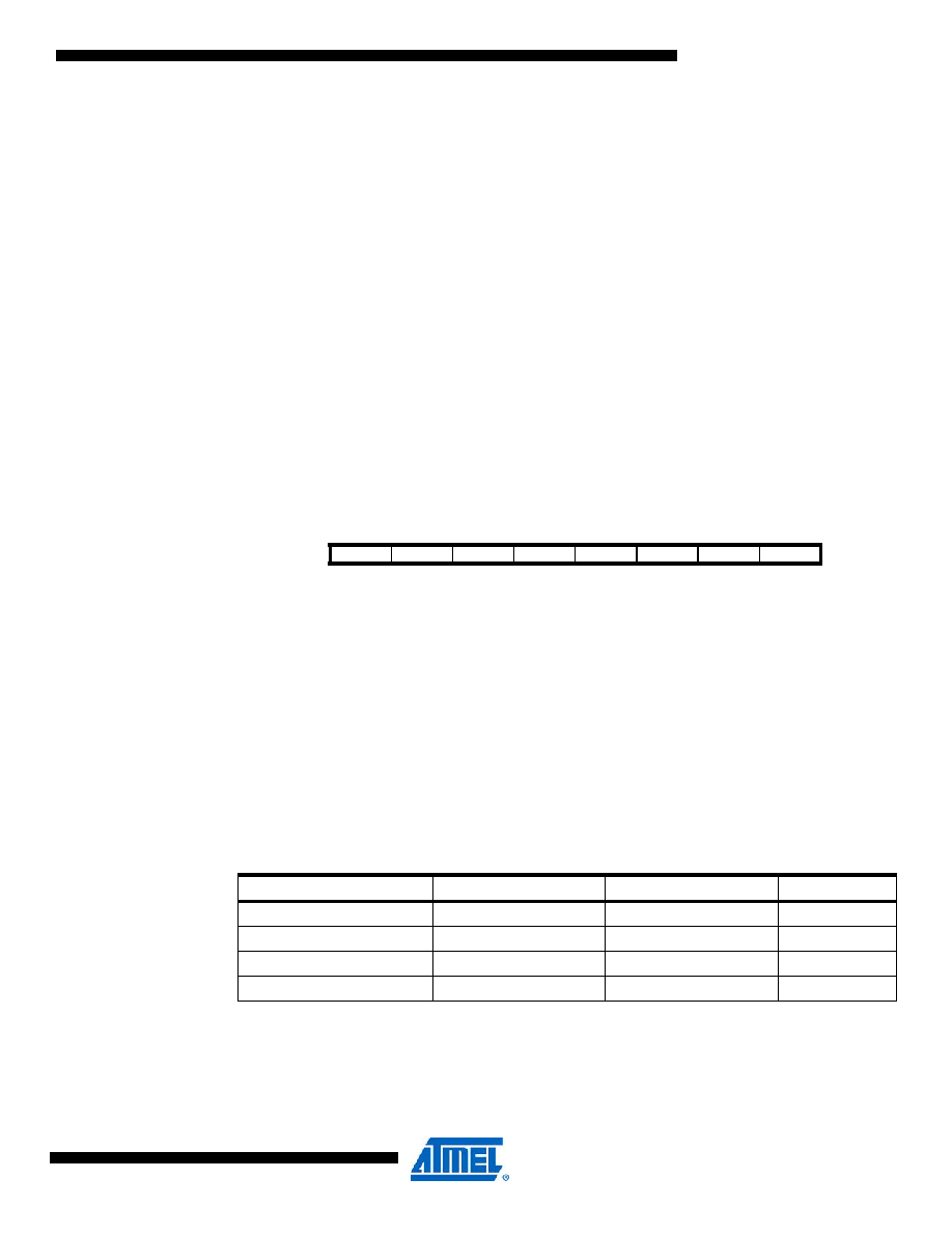
Bit
7
6
5
43
21
0
MSB
LSB
SPDR
Read/write
R/W
Initial value
X
Undefined
Table 18-5.
CPOL functionality.
Leading edge
Trailing edge
SPI mode
CPOL=0, CPHA=0
Sample (rising)
Setup (falling)
0
CPOL=0, CPHA=1
Setup (rising)
Sample (falling)
1
CPOL=1, CPHA=0
Sample (falling)
Setup (rising)
2
CPOL=1, CPHA=1
Setup (falling)
Sample (rising)
3
发布紧急采购,3分钟左右您将得到回复。
相关PDF资料
PIC18LF26K22-I/SP
IC PIC MCU 64KB FLASH 28SPDIP
PIC18F25K80-I/SP
MCU PIC 32KB FLASH 28SDIP
DSPIC33FJ12MC201-I/SS
IC DSPIC MCU/DSP 12K 20SSOP
PIC16LF628-04I/P
IC MCU FLASH 2KX14 COMP 18DIP
PIC16C716-04I/P
IC MCU OTP 2KX14 A/D PWM 18DIP
PIC18F26K22-I/SP
IC PIC MCU 64KB FLASH 28SPDIP
PIC18F45J11-I/PT
IC PIC MCU FLASH 32KB 44-TQFP
PIC24HJ12GP201-I/SO
IC PIC MCU FLASH 12KB 18SOIC
相关代理商/技术参数
PIC16C711-04/P
制造商:Microchip Technology Inc 功能描述:IC 8BIT CMOS MCU 16C711 DIP18
PIC16C711-04/SO
功能描述:8位微控制器 -MCU 1.75KB 68 RAM 13 I/O 4MHz SOIC18 RoHS:否 制造商:Silicon Labs 核心:8051 处理器系列:C8051F39x 数据总线宽度:8 bit 最大时钟频率:50 MHz 程序存储器大小:16 KB 数据 RAM 大小:1 KB 片上 ADC:Yes 工作电源电压:1.8 V to 3.6 V 工作温度范围:- 40 C to + 105 C 封装 / 箱体:QFN-20 安装风格:SMD/SMT
PIC16C711-04/SO
制造商:Microchip Technology Inc 功能描述:8BIT CMOS MCU SMD 16C711 SOIC18
PIC16C711-04/SS
功能描述:8位微控制器 -MCU 1.75KB 68 RAM 13 I/O 4MHz SSOP20 RoHS:否 制造商:Silicon Labs 核心:8051 处理器系列:C8051F39x 数据总线宽度:8 bit 最大时钟频率:50 MHz 程序存储器大小:16 KB 数据 RAM 大小:1 KB 片上 ADC:Yes 工作电源电压:1.8 V to 3.6 V 工作温度范围:- 40 C to + 105 C 封装 / 箱体:QFN-20 安装风格:SMD/SMT
PIC16C711-04E/P
功能描述:8位微控制器 -MCU 1.75KB 68 RAM 13 I/O 4MHz Ext Temp PDIP18 RoHS:否 制造商:Silicon Labs 核心:8051 处理器系列:C8051F39x 数据总线宽度:8 bit 最大时钟频率:50 MHz 程序存储器大小:16 KB 数据 RAM 大小:1 KB 片上 ADC:Yes 工作电源电压:1.8 V to 3.6 V 工作温度范围:- 40 C to + 105 C 封装 / 箱体:QFN-20 安装风格:SMD/SMT
PIC16C711-04E/SO
功能描述:8位微控制器 -MCU 1.75KB 68 RAM 13 I/O 4MHz Ext Temp SOIC18 RoHS:否 制造商:Silicon Labs 核心:8051 处理器系列:C8051F39x 数据总线宽度:8 bit 最大时钟频率:50 MHz 程序存储器大小:16 KB 数据 RAM 大小:1 KB 片上 ADC:Yes 工作电源电压:1.8 V to 3.6 V 工作温度范围:- 40 C to + 105 C 封装 / 箱体:QFN-20 安装风格:SMD/SMT
PIC16C711-04E/SS
功能描述:8位微控制器 -MCU 1.75KB 68 RAM 13 I/O 4MHz Ext Temp SSOP20 RoHS:否 制造商:Silicon Labs 核心:8051 处理器系列:C8051F39x 数据总线宽度:8 bit 最大时钟频率:50 MHz 程序存储器大小:16 KB 数据 RAM 大小:1 KB 片上 ADC:Yes 工作电源电压:1.8 V to 3.6 V 工作温度范围:- 40 C to + 105 C 封装 / 箱体:QFN-20 安装风格:SMD/SMT
PIC16C711-04I/P
功能描述:8位微控制器 -MCU 1.75KB 68 RAM 13 I/O 4MHz Ind Temp PDIP18 RoHS:否 制造商:Silicon Labs 核心:8051 处理器系列:C8051F39x 数据总线宽度:8 bit 最大时钟频率:50 MHz 程序存储器大小:16 KB 数据 RAM 大小:1 KB 片上 ADC:Yes 工作电源电压:1.8 V to 3.6 V 工作温度范围:- 40 C to + 105 C 封装 / 箱体:QFN-20 安装风格:SMD/SMT